A monocrystalline silicon material handling system is a specialized equipment designed to transport and manage monocrystalline silicon wafers or related materials within the semiconductor manufacturing process. These systems are critical in ensuring the efficient and precise movement of silicon wafers from one stage of production to another, such as from the growth or slicing stage to the polishing or testing stage. The design of these systems is tailored to meet the stringent requirements of the semiconductor industry, including high precision, low contamination, and the ability to handle delicate materials without damage.
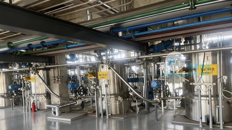
Key Design Principles of Monocrystalline Silicon Material Handling Systems
The design principles of monocrystalline silicon material handling systems are centered around several key factors that ensure optimal performance and reliability. First, the system must maintain a clean environment to prevent contamination of the silicon wafers, which are highly sensitive to particles and chemicals. This is achieved through the use of cleanroom technology, including HEPA filters, laminar flow hoods, and enclosed transport paths. Second, the system must provide precise positioning and alignment capabilities to ensure that the wafers are handled accurately, avoiding scratches or other damage that could affect their performance. This often involves the use of robotic arms, vacuum grippers, or precision conveyor systems that can move the wafers with sub-micron accuracy. Third, the system must be robust and durable to withstand the rigorous demands of continuous operation in a high-tech manufacturing environment. This includes the use of high-quality materials, such as stainless steel or specialized polymers, and robust mechanical components that can handle the weight and size of the silicon wafers. Finally, the system must be integrated with other production equipment to form a seamless workflow, ensuring that the wafers move efficiently through the entire manufacturing process without bottlenecks or delays.
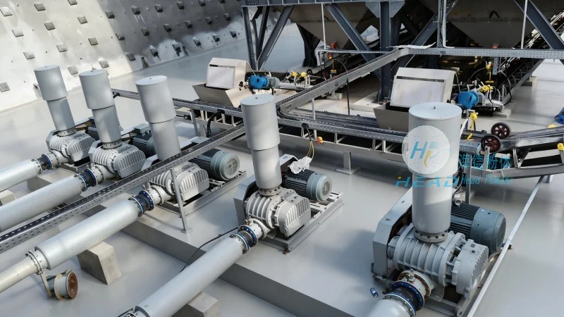
Components and Functionality of the Material Handling System
The monocrystalline silicon material handling system typically consists of several key components that work together to achieve its objectives. The primary components include a loading/unloading station, a conveyor or transport mechanism, a storage or buffer system, and a control system. The loading/unloading station is where the silicon wafers are loaded from the growth or slicing equipment and unloaded into the system. This station is equipped with specialized fixtures and vacuum grippers to securely hold the wafers during transport. The transport mechanism, which may include a conveyor belt, a roller system, or a robotic arm, moves the wafers from the loading station to the storage or processing areas. The storage system is designed to hold the wafers temporarily when they are not in use, ensuring that they are protected from contamination and damage. The control system uses sensors and software to monitor the position and status of the wafers, and to coordinate the movement of the system components. This system may also include feedback mechanisms to adjust the speed or direction of the transport based on the position of the wafers, ensuring precise handling.
Application and Benefits in Semiconductor Manufacturing
Monocrystalline silicon material handling systems are widely used in the semiconductor industry, particularly in the production of solar cells and integrated circuits. These systems play a crucial role in improving the efficiency and quality of the manufacturing process. By providing a reliable and precise method of transporting wafers, the system reduces the risk of damage and contamination, which can lead to defects in the final product. This, in turn, improves the yield of the manufacturing process, as fewer wafers are rejected due to quality issues. Additionally, the system enhances the overall productivity of the production line by ensuring that the wafers move quickly and efficiently from one stage to the next, minimizing downtime and bottlenecks. The use of advanced materials and cleanroom technology in the system also ensures that the wafers are handled in a way that maintains their high purity and quality, which is essential for the performance of the final semiconductor devices.
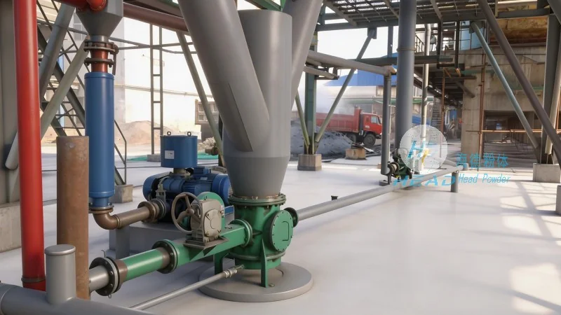
About HeadPowder Engineering
HeadPowder Engineering, a leading provider of specialized equipment for the semiconductor industry, is dedicated to delivering high-quality monocrystalline silicon material handling systems. With years of experience in the field, HeadPowder Engineering has developed a reputation for producing reliable and efficient systems that meet the stringent requirements of modern semiconductor manufacturing. The company's headquarters is located in Shandong, China, where it operates a state-of-the-art manufacturing facility equipped with the latest technology and skilled personnel. HeadPowder Engineering's commitment to quality and customer satisfaction has made it a trusted partner for many leading semiconductor manufacturers worldwide.